Distinct driving mechanisms for charge order in monolayer vanadium diselenide
February 24, 2022NUS physicists have discovered that monolayer vanadium diselenide (VSe2) has coexisting charge-ordered states with two distinct driving mechanisms.
Charge density waves (CDWs) are static modulations of electron density – typically occurring at a periodic interval of a few lattice constants in crystalline materials. Conventional CDWs occur within parallel regions of the electronic (“Fermi”) surface and are accompanied by a periodic (Peierls) modulation of the underlying atomic lattice.
Although known for nearly a century, CDWs continue to command considerable attention within the condensed matter physics community. The occurrence and tunability of CDWs in ultrathin two-dimensional (2D) materials are particularly interesting as these materials can also host other novel states (e.g. magnetism and superconductivity), and may be useful for electronic applications. The charge order in ultrathin materials with single or few-layers of atoms is also of fundamental interest, due to the increased significance of electron-electron interactions.
Vanadium diselenide (VSe2) in its monolayer form is a prototypical transition metal dichalcogenide. It has a conventional triangular CDW with periodicity of 4 times its lattice constant, 4a (where a is the lattice constant). However, the ground state of monolayer VSe2 is surrounded with controversy, with contrasting reports of ordered states of structural, electronic, and magnetic origin. Establishing the nature and origin of the charge order in monolayer VSe2 is important considering its use in potential applications, and in understanding the effects of strong coupling and correlations in ultrathin materials.
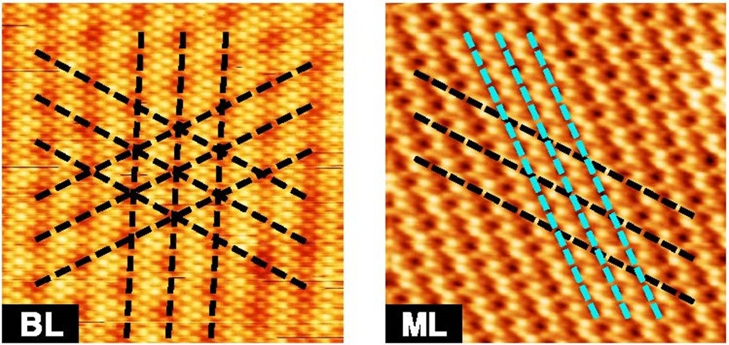
The research team led by Professor Andrew WEE and Assistant Professor Anjan SOUMYANARAYANAN both from the Department of Physics, National University of Singapore made significant progress in unravelling the nature and origin of the charge order found in monolayer VSe2. Their scanning tunnelling microscopy (STM) experiments establish that while the CDW in bilayer (BL)-VSe2 is closely related to the bulk material, it becomes qualitatively distinct in monolayer VSe2. Systematic studies across different substrates and temperatures reveal that monolayer VSe2 hosts two contrasting unidirectional CDWs, with periodicities of 4a and 2.8a respectively (see Figure). Their calculations show that, while the 4a CDW can be explained using the conventional Peierls mechanism, the 2.8a CDW cannot be explained within this framework. Instead, the researchers showed that this unconventional CDW may originate from strong electron-electron interactions. This research is a collaboration with the University of Amsterdam and the Indian Institute of Science.
Asst Prof Soumyanarayanan said, “Our findings have established monolayer VSe2 as the first material hosting two coexisting CDWs, each with a distinct driving mechanism. This work addresses the controversy surrounding the much-debated ground state of monolayer VSe2. It further paves the way for the use of emergent interactions to realise and tailor ordered states in ultrathin films and heterostructures, towards unconventional electronic devices.”

Figure shows the charge density waves imaged using scanning tunnelling microscopy for (left) bilayer (BL)-VSe2 and (right) monolayer (ML)-VSe2. Dashed colour-coded lines represent the wavefronts for the 4a (black) and 2.8a (cyan) charge density waves (CDWs) respectively. [Credit: ACS Nano]
Reference
Chua R; Henke J; Saha S; Huang YL; Gou J; He XY; Das T; van Wezel J*; Soumyanarayanan A*; Wee ATS*, “Coexisting Charge-Ordered States with Distinct Driving Mechanisms in Monolayer VSe2” ACS NANO DOI: 10.1021/acsnano.1c08304 Published: 2021.


