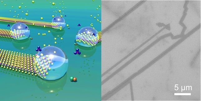
“The growth of ordered ribbons was a big surprise because the standard growth model does not predict such structures, but we realised that it was the result of a distinct growth mechanism,” said Dr LI, who was a research fellow in Prof Eda’s group but is now with the National Institute of Materials Science in Japan. The commonly accepted growth mechanism relies on the inherent dynamics of the precursors to diffuse and self-organise themselves on the substrate surface. Dr Li added, “This mechanism could not explain our observations.”
The researchers explain that the observed phenomenon is a form of the well-known vapour-liquid-solid (VLS) growth in which the vapour phase precursors condense into a liquid intermediate before forming the solid product. The morphology of the narrow ribbons obtained in this study was, however, unlike what is normally expected from a VLS growth, which typically yields cylindrical or tubular structures. Their observation indicates that the liquid droplet moves on the substrate surface in an ordered manner, leaving behind a track of ultrathin crystals. The process is similar to “painting with an ink droplet”.
The semiconducting ribbons synthesised by this method exhibited high crystal quality. The researchers demonstrated that high-performance microscopic transistors (with a field effect mobility of ~30 cm2/Vs and on-off ratio of ~106) can be fabricated from the individual ribbons. Because the as-synthesised material is already in the shape suitable for the device, this new growth method allows simple device fabrication without the need for an extra patterning step, which is normally required when other synthesis methods are used.
Prof Eda said, “Our work opens many interesting questions about surface and interface growth of nanomaterials. We believe that many other materials can be grown using a similar approach. The short-term goal is to understand the growth mechanism better and to control the morphology of the ribbons.”
Prof Eda envisions that the ability to directly grow complex semiconducting structures will greatly facilitate the realisation of high-performance nanoelectronic devices.

(Left) Visual showing the growth of molybdenum disulphide nanoribbons mediated by liquid nano-droplets. (Right) Electron microscopy image showing oriented molybdenum disulphide micro- and nano-ribbons.
Reference
S Li*; YC Lin; W Zhao; J Wu; Z Wang; Z Hu; Y Shen; DM Tang; J Wang; Q Zhang; H Zhu; L Chu; W Zhao; C Liu; Z Sun; T Taniguchi; M Osada; W Chen; QH Xu; ATS Wee; K Suenaga; F Ding; G Eda*, “Vapor-Liquid-Solid Growth of Monolayer MoS2 Nanoribbons” NATURE MATERIALS DOI: 10.1038/s41563-018-0055-z Published: 2018.


