NUS and BASF scientists open a way to high performance organic transistors for flexible electronics
Peter HO, CHUA Lay-Lay and PNG Rui-Qi ( (Group Leaders, Physics and Chemistry)) April 25, 201725 Apr 2017. NUS scientists in collaboration with BASF SE scientists have jointly developed a novel device structure for organic field-effect transistors (OFETs) that show unprecedentedly low contact resistance.
OFETs are envisaged in a wide variety of applications, ranging from electronic paper and wearable sensors, to distributed gadgets for the “Internet-of-Things”. They are switching devices that employ organic semiconductors, which are molecules or polymers comprising mainly carbon and hydrogen atoms, sometimes in combination with sulphur or oxygen atoms. These semiconductor materials are highly tailorable and inexpensive to deposit using solutions.
As the charge-carrier mobility of organic semiconductors, which measures how fast electrons (and holes) zip around in the material, reaches very high values, the performance of OFETs has become limited by resistance at the contact area between the metal and semiconductor layers. This resistance, called “contact resistance”, not only causes undesired heating and degradation of the contact, but also slows down the speed with which electrons (and holes) can get from one electrode to the other. This in turn slows down the frequency response of the device.
Now, in an article that has just been published in Advanced Functional Materials, NUS and BASF scientists report that this challenge can be overcome by incorporating a monolayer of a suitable polyelectrolyte, which is an ionic polymer, at the contact area to cause self-aligned doping of the adjacent semiconductor to a high density of electrons or holes, as desired. This produces a reliable contact with greatly reduced contact resistance, and works generally with different kinds of organic semiconductors. Contact resistance with values of less than 0.1 ohm cm2 have been realised, which is at least ten times lower than that without the monolayer.
Prof Lay-Lay CHUA, from the Department of Chemistry, who leads this innovation project, says, “This project is a collaboration between NUS scientists and BASF scientists to create chemistry that makes a difference in organic transistor technology. We believe the solution we have developed can also work with other types of advanced semiconductors of current interest, including carbon nanotubes.” A patent has been jointly filed by NUS and BASF. A process development roadmap is being put in place for product realisation using this technology.
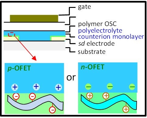
Figure shows a schematic structure of an n-channel OFET with self-aligned contact doping induced by a polyelectrolyte monolayer.
Reference
Seah WL; Tang CG; Png RQ; Keerthi V; Tan JK; Zhao C; Guo H; Yang JG; Zhou M; Ho PKH; Chua LL*, “Interface doping for ohmic organic semiconductor contacts using self-aligned polyelectrolyte counterion monolayer”, ADVANCED FUNCTIONAL MATERIALS DOI: 10.1002/adfm.201606291 Published: 2017.