Solution-processable conducting films with extreme work functions
Peter HO, CHUA Lay-Lay and PNG Rui-Qi ((Group Leaders, Physics and Chemistry) ) November 24, 201624 Nov 2016. NUS scientists in collaboration with scientists at Cambridge Display Technology Ltd (CDT), a subsidiary of Sumitomo Chemical Co., Ltd (SCC) have developed novel solution-processed conducting polymer materials with an unprecedented ultrawide range of work functions from 3.0 to 5.8 eV. These materials enable high quality, low resistance electrical contacts, called Ohmic contacts, to be attained for advanced semiconductor devices which are important for flexible electronics. This work was reported in Nature today.
The breakthrough is in the field of doped polymer organic semiconductors, which has been actively researched for nearly 30 years now. Organic semiconductors are made of carbon, hydrogen and other earth-abundant elements covalently bonded into molecules. When doped by chemical oxidation or reduction, mobile positive charges (holes) or negative charges (electrons), respectively, are introduced into the material, making it a good conductor of electricity.
The team led by Prof Peter HO and Dr Rui-Qi PNG from the Department of Physics, and Prof Lay-Lay CHUA from the Department of Chemistry, has shown that this process can be exploited to produce doped conducting polymer films with ultrahigh and ultralow work functions which are suitable for deployment in practical device structures by solution processing. Working with semiconducting polymers with bonded ionic groups, called conjugated polyelectrolytes, they show that the key is to employ strong charge doping together with an internal ion-exchange to remove free ions. This gives doped films with extreme work functions and enhanced stability against dedoping and dopant migration, the two most difficult challenges that the field has grappled with over the last decades. The resultant materials can be used as charge-injection layers to enhance the performance of a broad spectrum of devices, including organic light-emitting diodes, transistors, solar cells and photodiodes.
“This work originated from an agreement between our group at NUS and the CDT/ SCC team to develop hole- and electron-injection materials for organic electronics application. We are delighted that the project has led to a Singapore innovation of a general strategy for a new class of conducting polymers,” says Rui-Qi. “It also shows that materials with ultrahigh and ultralow work functions are important to make good electrical contacts for organic semiconductors and potentially other advanced semiconductors, including perovskites, two-dimensional (2D) materials, quantum dots and nanotubes.”
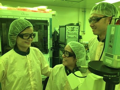
Image shows Dr Png Rui-Qi having a discussion with Ms Cindy TANG and Mr Mervin ANG in the laboratory.
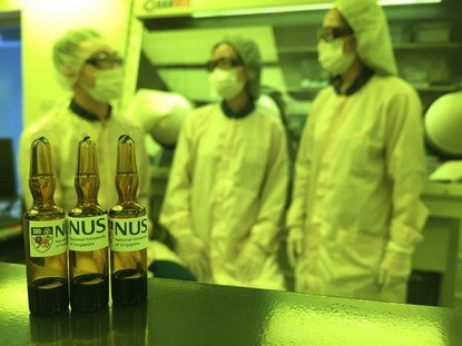
Image shows samples of ultralow work function doped polymer in ampoules in the foreground and Dr Png Rui-Qi and Mr Mervin Ang having a discussion in the background.
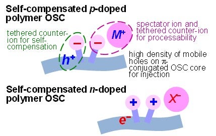
Schematic of self-compensated conducting polymers. The semiconducting polymer in the form of a conjugated polyelectrolyte with tethered counter-ion is hole (electron)-doped by a strong acceptor (donor), and then internally ion-exchanged to achieve the stable self-compensated state.
Reference
Tang CG; Ang MCY; Choo KK; Keerthi V; Tan JK; Nur Syafiqah M; Kulger T; Burroughes JH; Png RQ*; Chua LL*; Ho PKH*, “Doped polymer semiconductors with ultrahigh and ultralow work functions for ohmic contacts”, NATURE Volume: 539 Pages: 536-540 DOI: 10.1038/nature20133 Published: 2016