Unique photoresponse from 2D phosphorene-phosphorene-suboxide
SOW Chorng Haur (Group Leader, Physics) () June 02, 20162 Jun 2016. NUS physicists have observed special photoresponse behaviour from a new two-dimensional (2D) semiconductor.
Recently, few-layer black phosphorous (phosphorene) and its related phosphorene suboxide, a 2D semiconductor, was found to be a promising candidate for next generation nano-electronics and optoelectronics in the “post-graphene age”. The existence of the thickness-dependent direct band gap renders phosphorene an attractive candidate in optoelectronics. The ability to control the oxidation states of this phosphorene provides an additional handle to tailor the physical properties of this 2D system.
A team led by Prof Chorng Haur SOW, Prof Barbaros ÖZYILMAZ, Prof Antonio CASTRO-NETO, Dr Alexandra CARVALHO and Dr Junpeng LU from the Department of Physics and the Centre for Advanced 2D Materials in NUS devised a straightforward method to create a functional junction on a phosphorene flake, observing enhanced photoresponse from it.
The creation of a functional junction out of a phosphorene-based device is critical to transform these materials into functional devices. For example, a p-n junction was introduced into few-layer phosphorene through a complex electrostatic-doping method.The purpose is to realise the photovoltaic effect in phosphorene-based devices. The team in NUS demonstrates a much easier way to realise photovoltaic behaviour in phosphorene through the creation of a functional junction on a thin phosphorene flake in a two-probe device.Namely, with a simple focused laser beam, they can scan and convert a part of the phosphorene into phosphorene-suboxide species.
Given the functional and active phosphorene – a phosphorene suboxide junction in the device,the photoresponsivity and photocurrent distribution of the device can be significantly altered with qualitative difference in behaviour. It exhibits photovoltaic-like behaviour which is not found in a pristine sample!

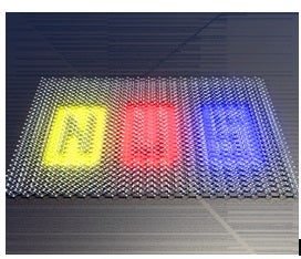
Figure depicts micro-patterning on few-layer black phosphorus by means of a scanning focused laser beam. [Image credit: Junpeng LU]
References
1. JP Lu, A Carvalho, J Wu, HW Liu, ES Tok, AH Castro-Neto, B. Özyilmaz, CH Sow. “Enhanced Photoresponse from Phosphorene-Phosphorene-Suboxide Junction Fashioned by Focused Laser Micromachining”, Advanced Materials, 2016, 28, 4090-4096 (Backcover Page Highlight).
2. JP Lu, J Wu, A Carvalho, A Ziletti, HW Liu, JY Tan, YF Chen, AH Castro-Neto, B. Özyilmaz, CH Sow. “Bandgap Engineering of Phosphorene by Laser Oxidation toward Functional 2D Materials” ACS Nano. 9 (2015) 10411.


