
“Butterfly” defects on 2D Materials
Andrew WEE (Group Leader, Physics) () June 20, 201620 Jun 2016. Scientists in NUS discovered novel defect states at grain boundaries (GBs) in a two-dimensional (2D) semiconductor.
Atomically thin 2D transition metal dichalcogenides (TMDs) such as tungsten diselenide (WSe2) are 2D semiconductors and therefore of interest for flexible electronic device applications. The presence of GBs can significantly influence their properties, but the direct imaging of these GB defects at the atomic scale remains extremely challenging.
A team led by Prof Andrew WEE and Prof QUEK Su Ying from the Department of Physics in NUS, together with Dr HUANG Yuli from A*STAR’s Institute of Materials Research and Engineering (IMRE) who did this work when she was a Research Fellow in NUS Physics, employ scanning tunnelling microscopy (STM) and spectroscopy to investigate the atomic and electronic structure of low-angle GBs of monolayer WSe2 with misorientation angles of 3−6°. Butterfly features corresponding to electronic gap states are observed along the GBs, with the periodicity depending on the misorientation angle.
From this study, the team have achieved a deeper understanding of the nature of GB defects. Such defects influence electronic transport and other device properties, and are therefore important in defect engineering for future 2D device applications.
Since the emergence of 2D materials, there has been intensive interest in defects as they strongly influence material properties. In particular, GBs are common in 2D crystals grown by bottom-up approaches such as chemical vapour deposition (CVD). A rich variety of GBs has been observed in graphene, hexagonal boron nitride (h-BN), as well as TMDs. GB defects can modify the properties of TMDs, including mechanical plasticity, chemical reactivity, electronic, optical, and magnetic properties. GBs need to be well understood as they can significantly influence the performance of electronic devices built on 2D materials.
The next step will be to control the large area growth of such 2D TMD materials such that either the defect density is reduced, or the specific properties of the defects are harnessed to enhance device applications.
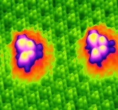
Figure shows an atomically-resolved scanning tunnelling microscopy image of dislocation defects in monolayer tungsten diselenide, where each green point represents a selenium atom. The background hexagonal Moire lattice is due to the graphite substrate. The dislocation defects feature as butterfly patterns in the 2D surface, arising from the electronic charge density redistribution at the atomic scale. [Image credit: Reprinted (adapted) with permission from Wee ATS, et.al., “Gap States at Low-Angle Grain Boundaries in Monolayer Tungsten Diselenide”, Nano Letters 16 (2016). Copyright 2016 American Chemical Society.]
Reference
Huang YL, Ding Z, Zhang W, Chang YH, Shi Y, Li LJ, Song Z, Zheng YJ, Chi D, Quek SY, Wee ATS. “Gap States at Low-Angle Grain Boundaries in Monolayer Tungsten Diselenide”. Nano Letters 16 (2016) DOI: 10.1021/acs.nanolett.6b00888