Scientists in Singapore develop novel ultra-fast electrical circuits using light-generated tunneling currents
Christian NIJHUIS ( Group Leader, Chemistry) () April 09, 20149 April 2014
Scientific breakthrough to potentially revolutionise high-speed electronics, nanoscale opto-electronics and nonlinear optics
8 April 2014, Singapore – Assistant Professor Christian A. Nijhuis of the Department of Chemistry at the National University of Singapore’s (NUS) Faculty of Science, in collaboration with researchers from the Agency for Science, Technology and Research (A*STAR), namely Dr Bai Ping of the Institute of High Performance Computing and Dr Michel Bosman of the Institute of Materials Research and Engineering has successfully designed and fabricated electrical circuits that can operate at hundreds of terahertz frequencies, which is tens of thousands times faster than today’s state-of-the-art microprocessors.
This novel invention uses a new physical process called ‘quantum plasmonic tunnelling’. By changing the molecules in the molecular electronic device, the frequency of the circuits can be altered in hundreds of terahertz regime. The new circuits can potentially be used to construct ultra-fast computers or single molecule detectors in the future, and open up new possibilities in nano-electronic devices. The study is funded by the National Research Foundation (NRF) and A*STAR and results of the research were first published in prestigious scientific journal Science on 28 March 2014.
The quest to be super-small and super-fast
Light is used as an information carrier and transmitted in optical fibre cables. Photonic elements are large but they operate at extremely high frequencies of 100 terahertz – about 10,000 times faster than the desktop computer. But current state-of-the-art nano-electronic devices operate at length scales that are much smaller, making it very difficult to combine the ultra-fast properties of photonic elements with nano-scale electronics.
Scientists have long known that light can interact with certain metals and can be captured in the form of plasmons, which are collective, ultra-fast oscillations of electrons that can be manipulated at the nano-scale. The so-called quantum plasmon modes have been theoretically predicted to occur at atomic length scales. However, current state-of-the-art fabrication techniques can only reach length scales that are about five nanometre larger, therefore quantum-plasmon effects have been difficult to investigate.
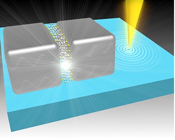
In this landmark study, the research team demonstrated that quantum-plasmonics is possible at length scales that are useful for real applications. Researchers successfully fabricated an element of a molecular electronic circuit using two plasmonic resonators, which are structures that can capture light in the form of plasmons, bridged by a layer of molecules that is exactly one molecule thick. The layer of molecules switches on the quantum plasmonic tunneling effects, enabling the circuits to operate at terahertz frequencies.
Dr Bosman used an advanced electron microscopy technique to visualise and measure the opto-electronic properties of these structures with nanometer resolution. The measurements revealed the existence of the quantum plasmon mode and that its speed could be controlled by varying the molecular properties of the devices.
By performing quantum-corrected simulations, Dr Bai confirmed that the quantum plasmonic properties could be controlled in the molecular electronic devices at frequencies 10,000 times faster than current processors.
Explaining the significance of the findings, Asst Prof Nijhuis said, “We are very excited by the new findings. Our team is the first to observe the quantum plasmonic tunneling effects directly. This is also the first time that a research team has demonstrated theoretically and experimentally that very fast-switching at optical frequencies are indeed possible in molecular electronic devices.”
The results open up possible new design routes for plasmonic-electronics that combines nano-electronics with the fast operating speed of optics.
Further research
To further their research, Asst Prof Nijhuis and his team will look into resolving the challenges that are presented in the course of their work, such as the integration of these devices into real electronic circuits. They are also following up with new ideas that are developed from these results.

A focused electron beam (in yellow) was used to characterise the structures and to probe the optical properties of two plasmonic resonators bridged by a layer of molecules with a length of 0.5 nm. (Image credit: Tan Shu Fen, National University of Singapore)
– End –
For media inquiries, please contact the NUS Media Relations team.


